DDR3 Layout Guidelines: Essential Tips for PCB Design Switched-mode power supply pcb design guidelines
If you are looking for PCB Design Rules and Tips you've visit to the right web. We have 25 Images about PCB Design Rules and Tips like PCB layout guidelines and considerations, High Speed Pcb Layout Guidelines - Design Talk and also Essential Guidelines For PCB Silkscreen For The Layout. Read more:
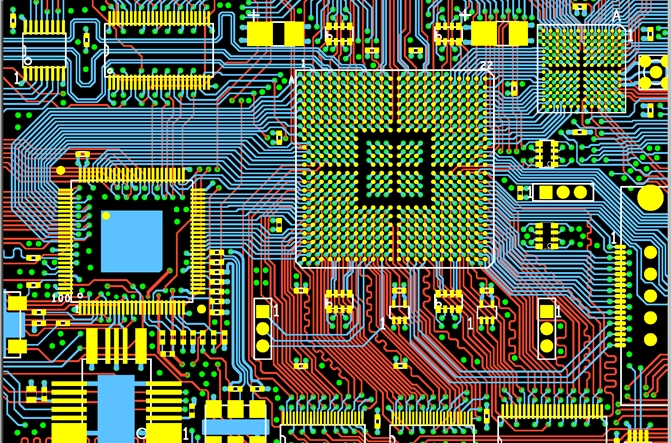
PCB Design Rules And Tips
 www.6pcb.com
PCB Design Rules and Tips
Pcb Routing Guidelines - Design Talk
 design.udlvirtual.edu.pe
Pcb Routing Guidelines - Design Talk
An520 DDR3 SDRAM Memory Interface Termination And Layout Guidelines
 www.scribd.com
an520 DDR3 SDRAM Memory Interface Termination and Layout Guidelines ...
High Speed Pcb Layout Guidelines - Design Talk
 design.udlvirtual.edu.pe
High Speed Pcb Layout Guidelines - Design Talk
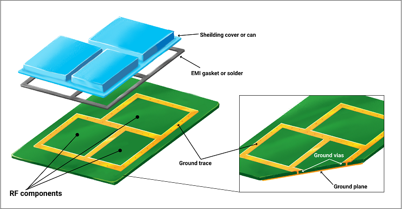
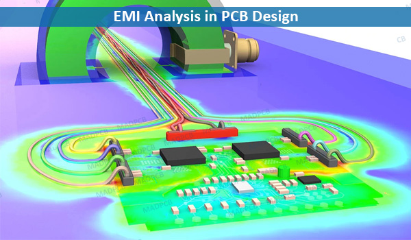
7 Tips And PCB Design Guidelines For EMI And EMC
 www.coder96.com
7 Tips and PCB Design Guidelines for EMI and EMC
Tips And Tricks To Build Efficient 433mhz PCB Antenna Design - RayPCB
 www.raypcb.com
Tips and Tricks to Build Efficient 433mhz PCB Antenna Design - RayPCB
China A1 A2 Sodimm Ddr4 Pcb Layout Guidelines Ddr3 Ram Pcb Design 2.0mm
 www.chinax.com
China A1 A2 Sodimm Ddr4 Pcb Layout Guidelines Ddr3 Ram Pcb Design 2.0mm ...
Main Design Guidelines & Layout Rules On High Speed PCB
 www.integrasources.com
Main Design Guidelines & Layout Rules on High Speed PCB
Main Design Guidelines & Layout Rules On High Speed PCB
 www.integrasources.com
Main Design Guidelines & Layout Rules on High Speed PCB
Pcb Design Tips At Marjorie Hiller Blog
 storage.googleapis.com
Pcb Design Tips at Marjorie Hiller blog
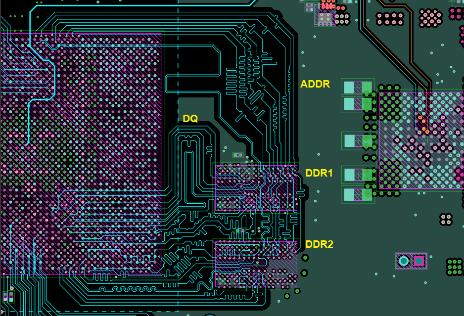
Ddr3 Layout Guidelines - Diysens
 diysens.blogspot.com
Ddr3 Layout Guidelines - Diysens
Ten Golden Rules Of PCB Design & Its Guidelines - AES
 absolutepcbassembly.com
Ten Golden Rules of PCB Design & its Guidelines - AES
PCB Layout Optimization For EMI And EMC
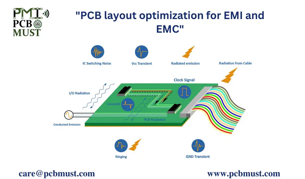 pcbmust.com
PCB Layout Optimization for EMI and EMC
Component Placement In PCB Design & Assembly | Sierra Circuits
 www.protoexpress.com
Component Placement in PCB Design & Assembly | Sierra Circuits
Xilinx Spartan-6 FPGA DDR3 Signal Integrity Analysis And PCB Layout
 www.scribd.com
Xilinx Spartan-6 FPGA DDR3 Signal Integrity Analysis and PCB Layout ...
What Is High Speed PCB Design - Guidelines And Best Practice Tips - IBE
 www.pcbaaa.com
What is high speed PCB design - guidelines and best practice tips - IBE ...
Section II. PCB Layout Guidelines
 www.yumpu.com
Section II. PCB Layout Guidelines
China A1 A2 Sodimm Ddr4 Pcb Layout Guidelines Ddr3 Ram Pcb Design 2.0mm
 www.chinax.com
China A1 A2 Sodimm Ddr4 Pcb Layout Guidelines Ddr3 Ram Pcb Design 2.0mm ...
High Current Pcb Design Guidelines - Design Talk
 design.udlvirtual.edu.pe
High Current Pcb Design Guidelines - Design Talk
PCB Layout Guidelines And Considerations
 www.microcontrollertips.com
PCB layout guidelines and considerations
Switched-Mode Power Supply PCB Design Guidelines | Altium
 resources.altium.com
Switched-Mode Power Supply PCB Design Guidelines | Altium
PCB Layout Support - Embizon Technologies - PCB Design Services, Bangalore
 www.embizon.com
PCB Layout Support - Embizon Technologies - PCB Design Services, Bangalore
PCB Design Guidelines For EMI EMC - RayMing PCB
 www.raypcb.com
PCB Design Guidelines For EMI EMC - RayMing PCB
Essential Guidelines For PCB Silkscreen For The Layout
 www.sunstreamglobal.com
Essential Guidelines For PCB Silkscreen For The Layout
The Essential Guide To PCB Heatsink Design And Selection - RayPCB
 www.raypcb.com
The Essential Guide to PCB Heatsink Design and Selection - RayPCB
Essential guidelines for pcb silkscreen for the layout. The essential guide to pcb heatsink design and selection. Switched-mode power supply pcb design guidelines